Screen Replacement
2024-10-18
Overview
Original 10.4” TFT (Sharp LQ10D016) was dead on arrival. Electrolyte leakage from aging caps corroded the ribbon cables to the driver ICs. Extremely common with these machines. No OEM replacement exists, Sharp won’t release the datasheet. Had to find a modern 10.4” 640×480 TFT and make it work.
Original Display: Sharp LQ10D016
No official datasheet for the LQ10D016. The pinout was reverse-engineered by Beckenrandschwimmer on DOSReloaded. Probed the video card output with an oscilloscope and test patterns to map every signal. This project wouldn’t have happened without that work. Closest available datasheet is the Sharp LQ10D011, same 3-bit-per-channel color architecture, same horizontal display start at clock 144, identical timing. The LQ10D011 uses a 22-pin interface (CN1) vs the Compaq’s custom 30-pin ribbon, but the signals and timing match. Between the LQ10D011 datasheet and Beckenrandschwimmer’s scope work, I had a complete picture. See LQ10D011 Datasheet (PDF).
Key characteristics of the original display:
| Parameter | Value |
|---|---|
| Model | Sharp LQ10D016 |
| Size | 10.4” diagonal |
| Resolution | 640×480 |
| Color depth | 3-bit per channel (9-bit total, 512 colors) |
| Backlight | Heated-cathode fluorescent tubes (HCFT) |
| Sync method | H-Sync + V-Sync (no Data Enable) |
| H-Sync display start | Clock 144 |
| Video modes | 480 lines (60 Hz), 400 lines (70 Hz), 350 lines (70 Hz) |
| Pixel clock | 25.175 MHz |
My Replacement: Sharp LQ104V1DG51
After a lot of searching and trial and error, I went with a Sharp LQ104V1DG51. See LQ104V1DG51 Datasheet (PDF). Originally I wanted a panel with a fixed horizontal display start at clock 144 matching the Compaq’s video card timing. That would have avoided the delay circuit entirely. No such panel exists, or if it does, it doesn’t support 400-line and 350-line DOS modes.
The LQ104V1DG51 was the best compromise. Natively supports 480-line, 400-line, and 350-line modes. Mode selection is via H-Sync/V-Sync polarity, which is exactly how the Compaq signals it. All three DOS modes work without extra circuitry. Trade-off: I need the BLANK-to-DE delay circuit for horizontal alignment.
| Mode | H-Sync | V-Sync |
|---|---|---|
| 480 lines | Negative | Negative |
| 400 lines | Negative | Positive |
| 350 lines | Positive | Negative |
Beckenrandschwimmer successfully used a Sharp LQ10D421, and a third person used an LQ104V1DG11. The approach is the same for all of these.
Key Differences from the Original
| Original (LQ10D016) | Replacement (LQ104V1DG51) | |
|---|---|---|
| Connector | Proprietary 30-pin (undocumented) | Standard 31-pin TTL |
| Color depth | 3-bit/channel (512 colors) | 6-bit/channel (262,144 colors) |
| Backlight | HCFT (heated cathode), 12V supply | CCFL (cold cathode), 5V supply |
| Data Enable | Not required | Required (ENAB pin 27) |
| H-Sync display start | Clock 144 | Clock 104 |
Challenges
Problems I had to solve:
- Proprietary 30-pin connector. No documentation. Pinout had to be reverse-engineered. New display uses standard 31-pin, so I needed an adapter cable.
- 40-pixel horizontal shift. New display starts drawing 40 clocks early, image shifts left.
- No Data Enable signal. Video card doesn’t output DE, new display requires it.
- Color depth mismatch. Video card outputs 3 bits per color, new display expects 6-8 bits.
- Backlight incompatibility. Completely different inverter requirements.
- 70 Hz DOS modes. Most new displays can’t handle 400-line/70 Hz and 350-line/70 Hz. Image wraps at the bottom. The panel I found supports it.
Pin Mapping
Full pin-by-pin mapping is in Compaq Display Pinout Mapping (PDF).
Key wiring notes:
- Original 3 color bits per channel (RED LSB/RED/RED MSB) map to the upper 3 bits of the new 6-bit channels (R3-R5, G3-G5, B3-B5). Lower bits (R0-R2, G0-G2, B0-B2) tied to GND.
- Pin 28 on the old connector was unused. Lucky. That’s where I route the generated Data Enable signal.
- H-Sync (old pin 4) and V-Sync (old pin 6) connect straight through.
- Dot Clock (old pin 2, 25 MHz) to DCLK (new pin 2).
- Power: old pin 7/8 (+5V) to new pin 28/29 (VCC). Old pin 30 (+12V) not needed.
Adapter Cable
New display has standard 31-pin TTL, Compaq outputs through a proprietary undocumented 30-pin ribbon cable. Can’t plug one into the other. Rather than hand-soldering 30 wires, I grabbed a 40-pin to 31-pin TTL LVDS cable with a breakout board (eBay item 173579595077). Could have custom made one for exactly 30 pins, but this was off the shelf and it works. 31-pin end plugs into the new display, breakout board side I soldered to the Compaq’s original ribbon connector.
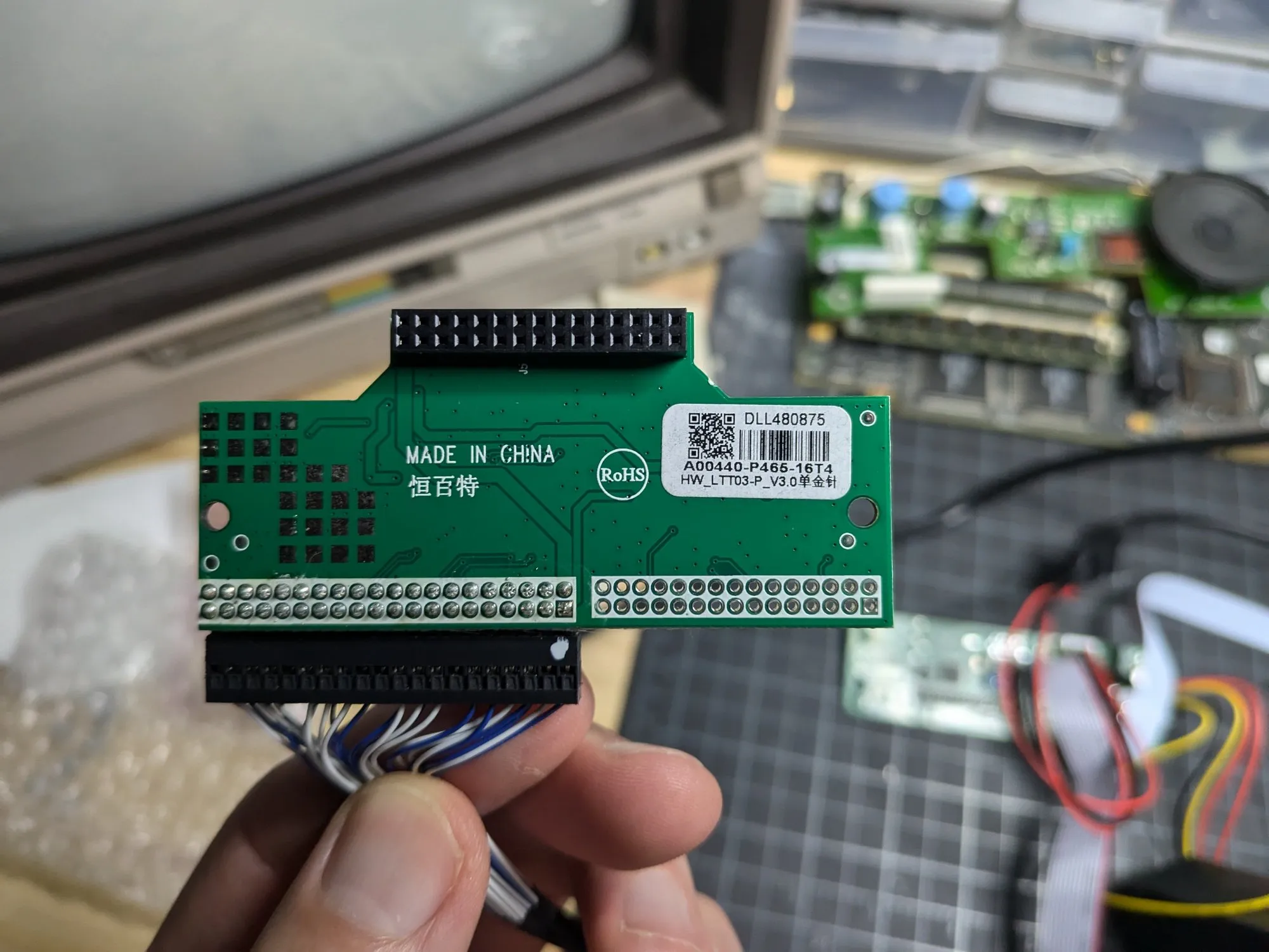
Full 40-pin connector pinout →
Data Enable / Horizontal Alignment Circuit
New display needs a Data Enable (DE) signal and starts drawing at clock 104 instead of 144. That’s a 40-pixel horizontal offset. The fix (originally from Beckenrandschwimmer on DOSReloaded) uses the BLANK signal from the RAMDAC as a delayed Data Enable.
The Problem
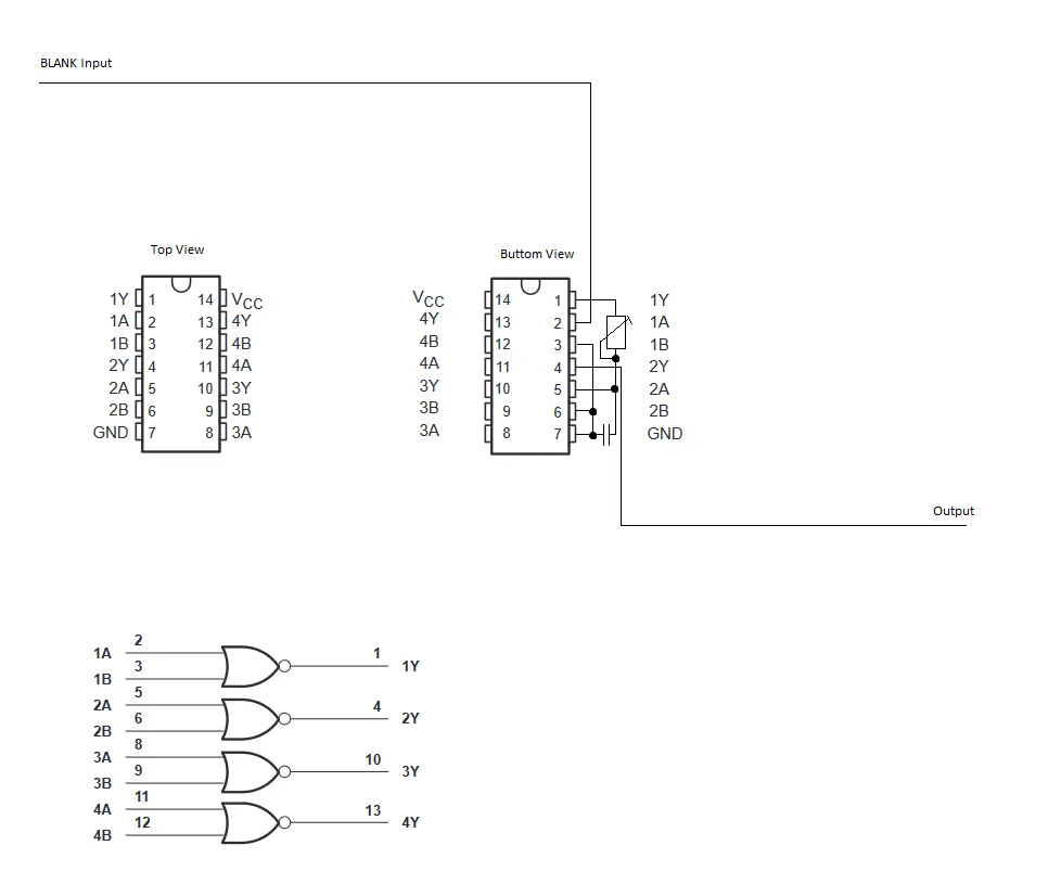
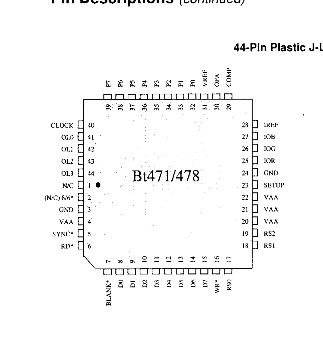
The Compaq’s Cirrus Logic video controller outputs H-Sync, V-Sync, and a BLANK signal from the RAMDAC. Video card uses a Brooktree Bt47x series RAMDAC (Bt471/476/478 family). BLANK* is at pin 7 on the 44-pin PLCC package. TTL-compatible, active-low. See BT471 RAMDAC Datasheet (PDF).
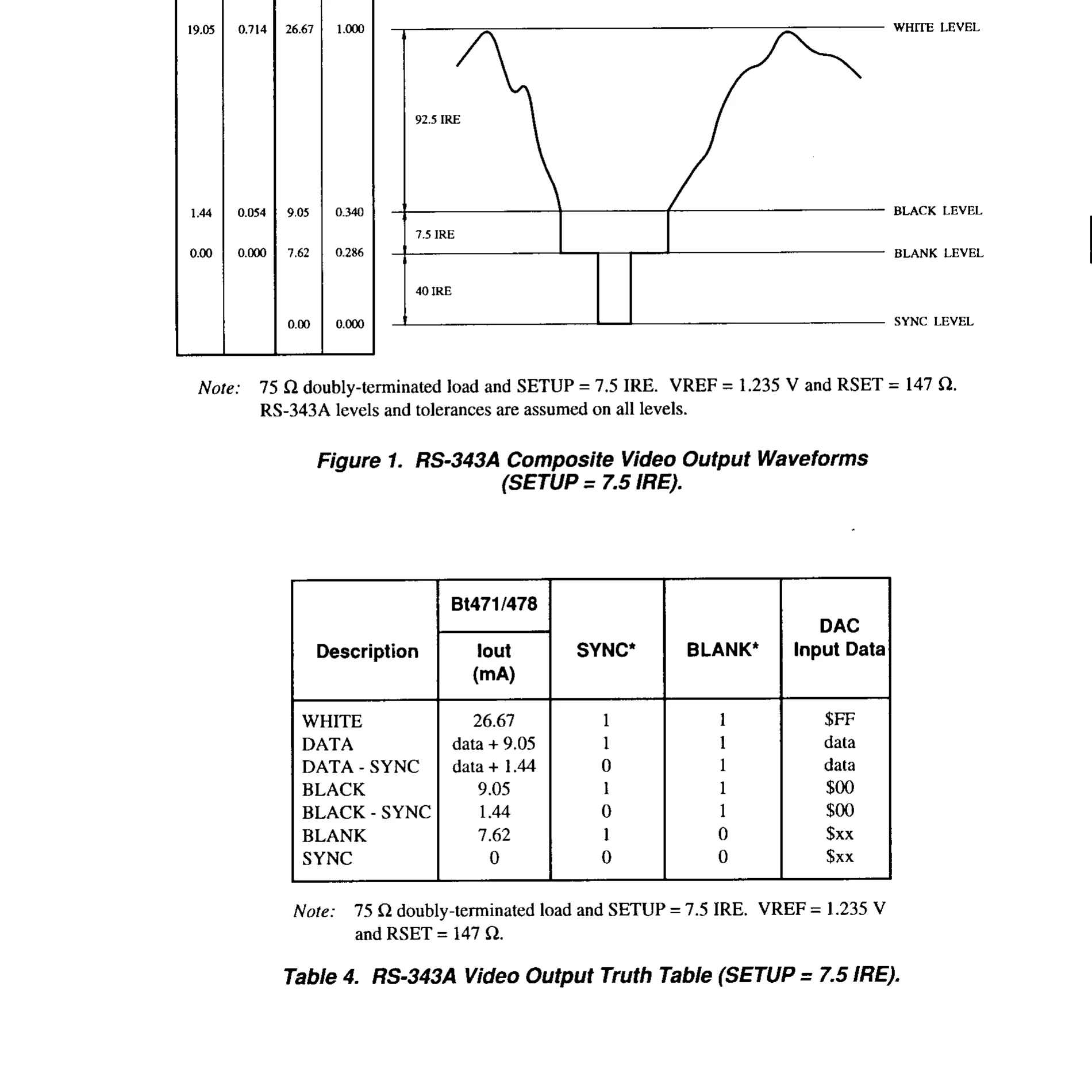
BLANK* = 1 during active display (pixel data visible), BLANK* = 0 during blanking intervals and sync. That’s the signal we need. Invert and delay it to get Data Enable.
Original display used H-Sync and V-Sync directly for pixel positioning, fixed start at clock 144 after H-Sync. Modern displays want a DE signal that goes high during active display instead. My new display expects pixels at clock 104. Compaq sends them at 144. Need to delay DE by exactly 40 clocks (~1.58 µs at 25.175 MHz) to line things up.
RC Delay Approach
Simple RC delay network between two inverter stages. BLANK* from the RAMDAC is active-low during blanking; when high, display is in the active region (see truth table above). Invert it, delay through the RC network, invert again. Out comes a properly timed DE signal.
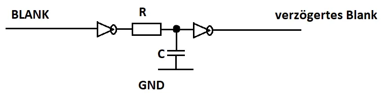
Delay is set by the RC time constant: τ = R × C. 10 kΩ trimmer pot and 22 pF cap covers the ~1.58 µs I need. Turning the trimmer shifts the image left or right, pixel by pixel.
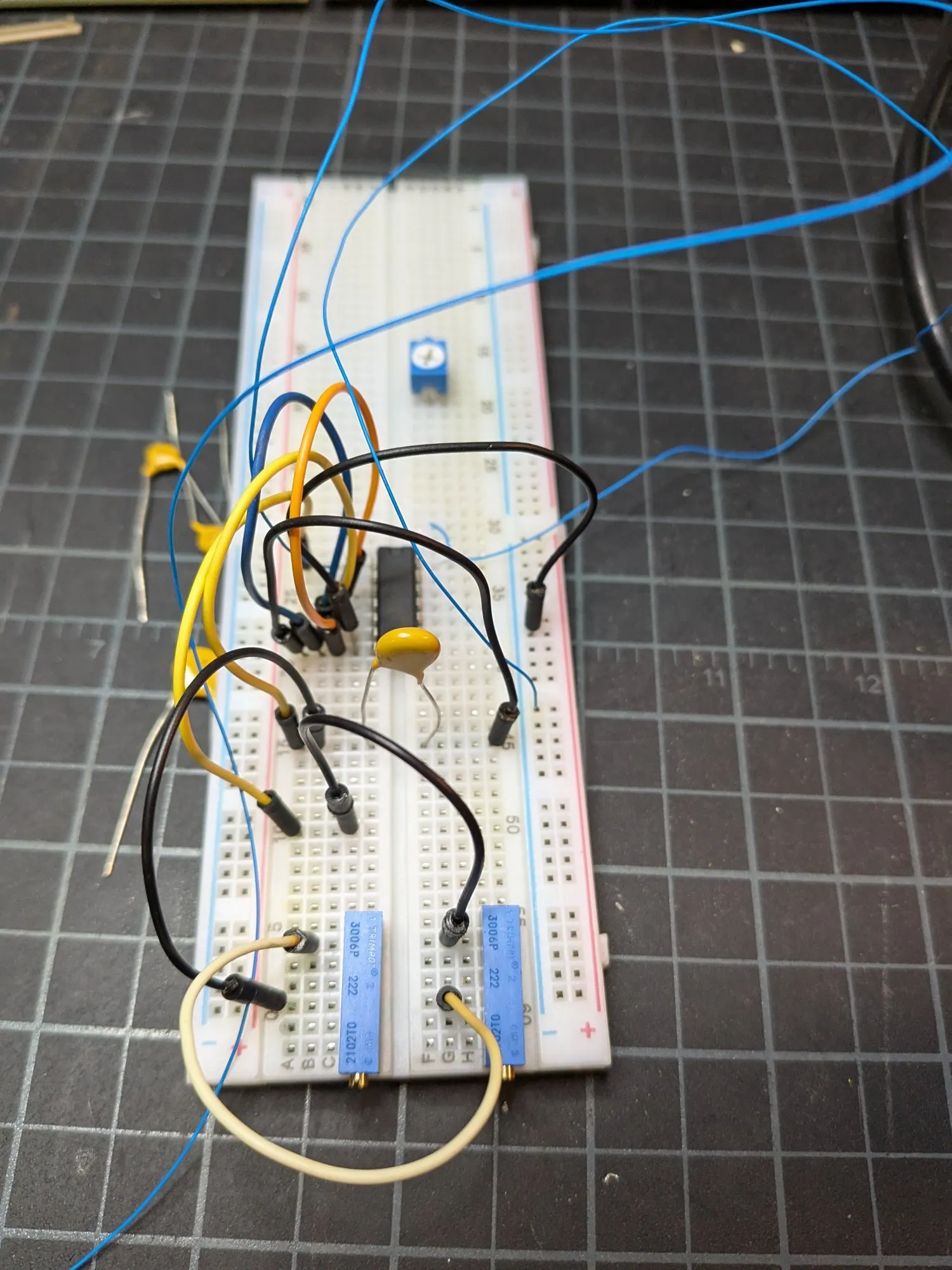
74AS02 NOR Gate Implementation
SN74AS02N, quad 2-input NOR gate. Tie both inputs together and a NOR gate acts as an inverter. I use two of the four gates as the inverter stages. Other two are unused (inputs tied to GND per standard practice).
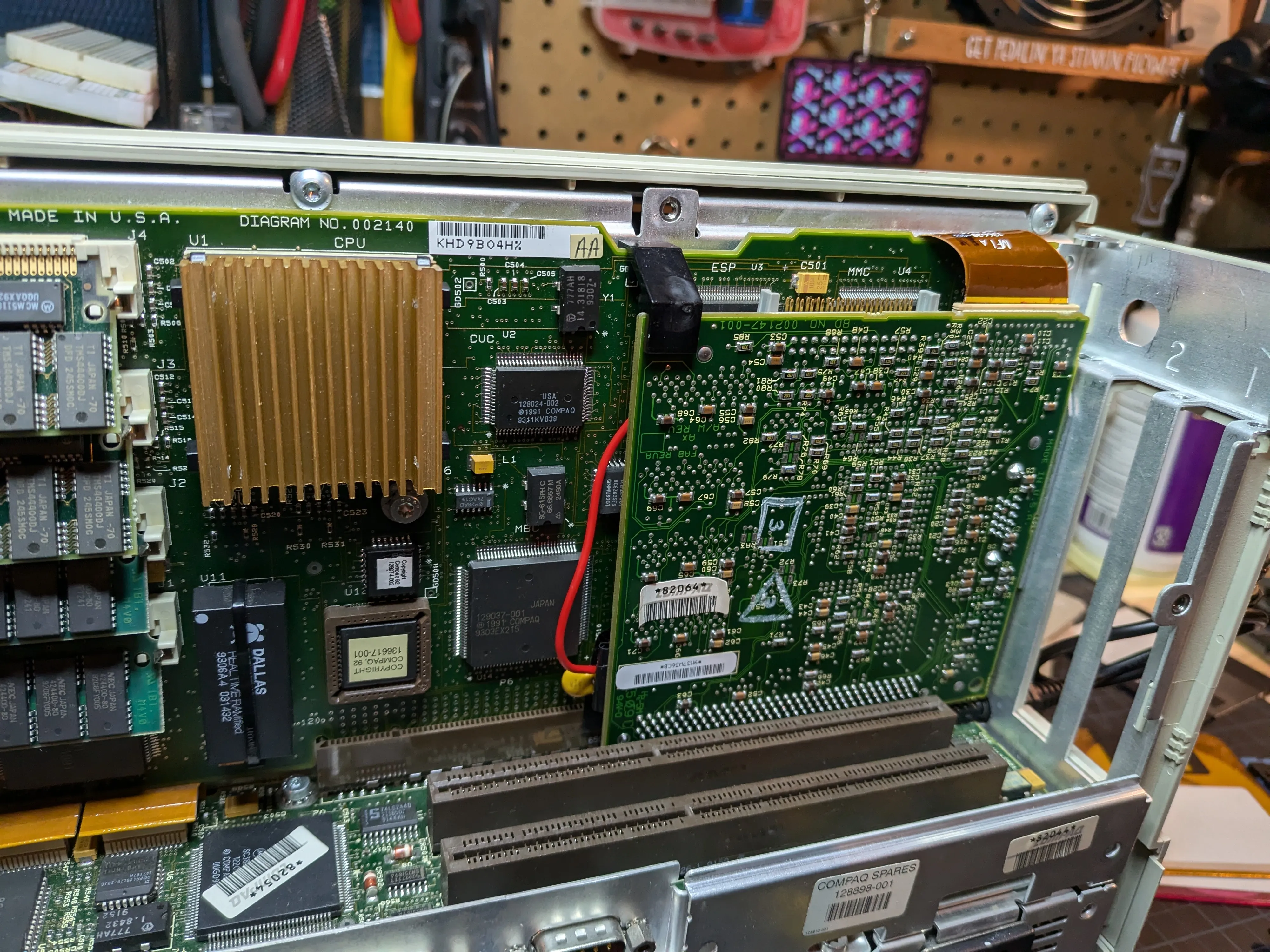
Physical wiring on the video card. The 74AS02 is soldered dead-bug style (upside down) directly onto the PCB.
Key connections:
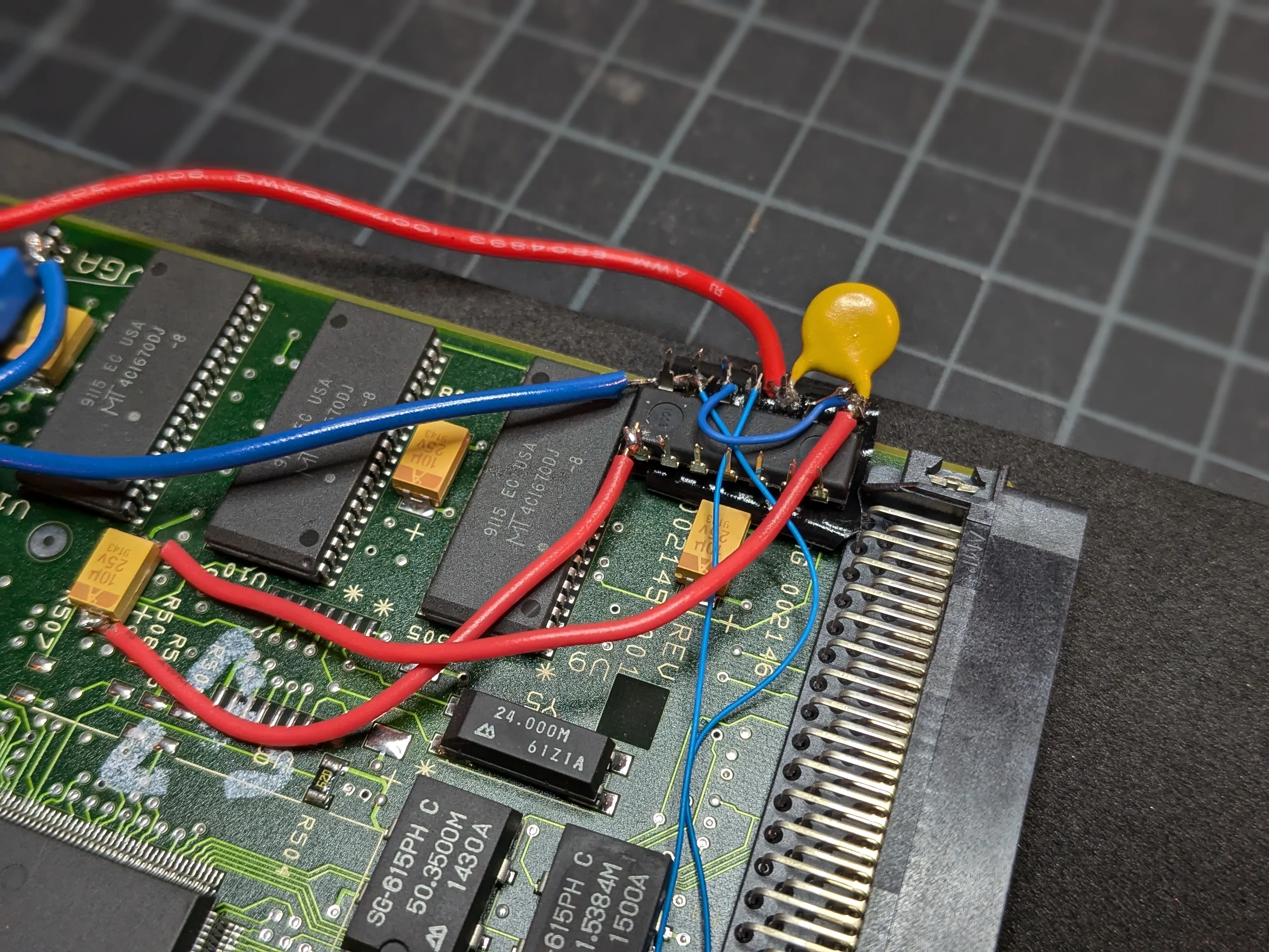
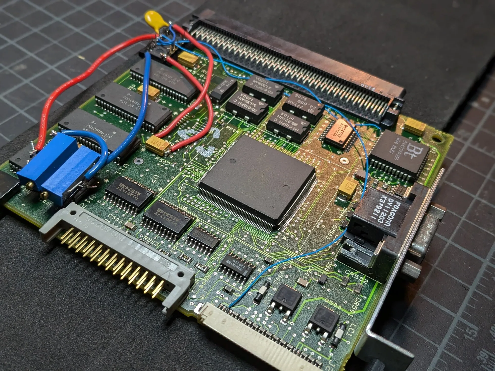
- BLANK input is tapped from pin 7 (BLANK*) on the Bt47x RAMDAC on the video card with a wire
- Gate 1 (pins 2+3 → pin 1): Both inputs tied to BLANK. Output is inverted BLANK.
- RC network: Connected between Gate 1 output (pin 1) and Gate 2 input. The trimmer pot (R) and capacitor (C) to GND create the adjustable delay.
- Gate 2 (pins 5+6 → pin 4): Both inputs tied to the delayed signal. Output is the final DE signal, now re-inverted and delayed.
- Pin 14 (VCC): +5V power
- Pin 7 (GND): Ground
- Output (pin 4): Routed to the unused pin 28 of the original 30-pin display cable, which connects to the DE input on the new display.
Went with “Advanced Schottky” (AS) for the fast propagation delay (~1.5 ns). Keeps the DE edges sharp at 25 MHz pixel clock. Standard 74LS or 74HC would add too much delay and degrade the edges.
Components
| Part | Value | Notes |
|---|---|---|
| IC | SN74AS02N | Quad 2-input NOR gate, two gates used as inverters |
| C1 | 22 pF | Timing capacitor (150 pF also works but gives coarser adjustment) |
| R1 | Bourns 3006P-1-222LF (2.2 kΩ) | Precision multi-turn trimmer pot, fine-tunes the delay to align the image horizontally (Mouser) |
| C_bypass | 220 nF ceramic | Decoupling cap directly across IC VCC/GND pins |
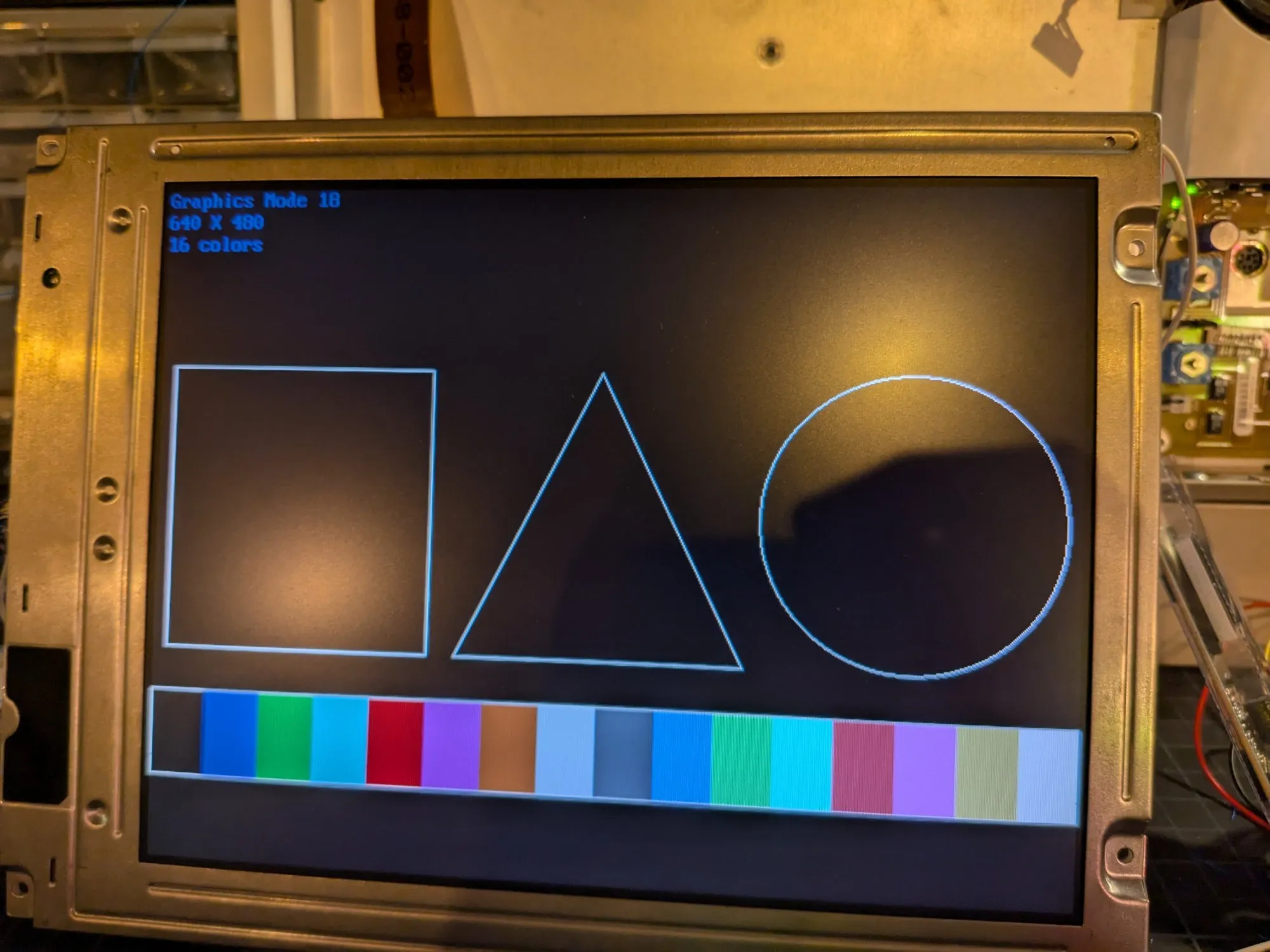
Calibration
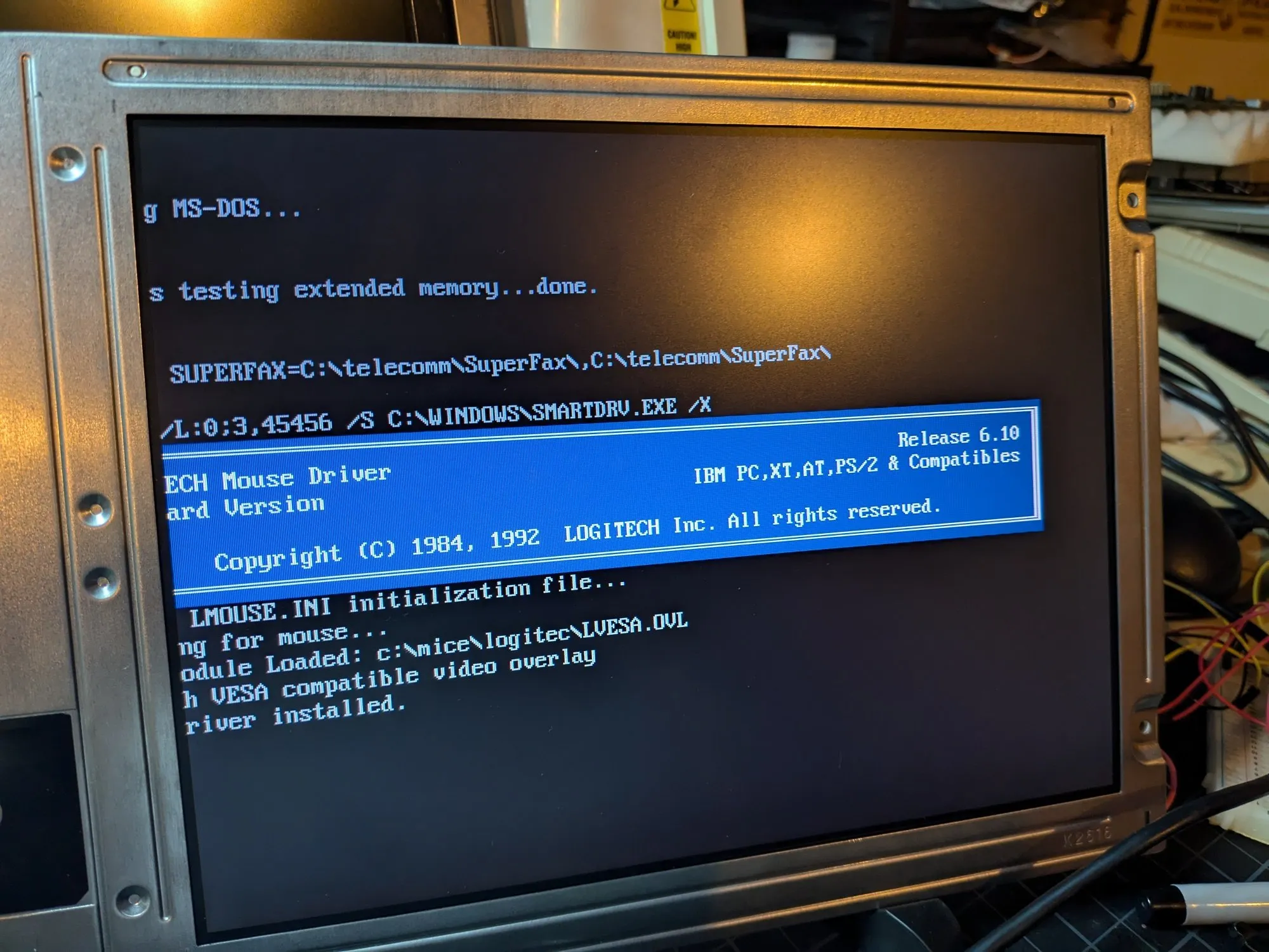
- Boot the machine to a known pattern (a DOS text prompt works fine, the left edge of the
C:\>cursor is a clean vertical reference) - Adjust the trimmer slowly until the image is centered in the display with no black bar on either side
- The delay is approximately 1.58 µs for the 40-pixel offset at 25.175 MHz
My Implementation Notes
Used two trimmer pots instead of one. When I first prototyped this the signal wasn’t clean and I needed finer tuning, so I kept both. One pot for the main RC delay, second for fine-tuning. Both visible in the photos below.
For +5V and GND, I probed the video card with a multimeter to find solid tap points near where the 74AS02 sits. Yellow 220 nF ceramic disc bypass cap is soldered directly across VCC and GND (pin 14 and pin 7).
Placed everything near the bottom where the case exhaust fan pushes air.
My PSU was already rebuilt so I had clean 5V available. Simplified things vs the DOSReloaded approach where they tapped 12V and regulated down with an LM78L05 because the 5V rail had too much ripple.
If your 5V rail is noisy (common with original PSUs), follow the DOSReloaded approach:
- Tap the 12V rail and regulate down to 5V with an LM78L05
- 10Ω resistor + 1000 µF cap before the regulator input
- 470 µF cap on the output
- Reverse-biased protection diode across the regulator output
Regardless of your 5V source:
- 220 nF bypass cap directly across the IC power pins is mandatory (not in my pics, it was added later)
- Mount the IC away from heat sources; temperature drift can shift the image up to 4 pixels
Backlight
Original HCFT inverter won’t work with the CCFL tubes in the new display. Wired in a modern dual CCFL inverter board (eBay item 405140078781) off the 12V supply from the original inverter board.
TODO: Wire the new inverter’s dimmer input to the Compaq’s front-panel brightness potentiometer. Currently brightness is not adjustable from the front panel.
TODO: Track down the exact inverter model number and datasheet, and take photos of the installed inverter board.
Note: The DOSReloaded build used a CCFL Driver 104PW201, which conveniently accepts a 10kΩ pot matching the original. That approach gives front-panel brightness control out of the box.
Physical Mounting
LQ104V1DG51 is much slimmer than the original because modern CCFL vs bulky heated-cathode tubes. Doesn’t fill the display cavity. Superglued it in. Not elegant, but it holds.
TODO: Add photos of the display mounted in the case.
Results
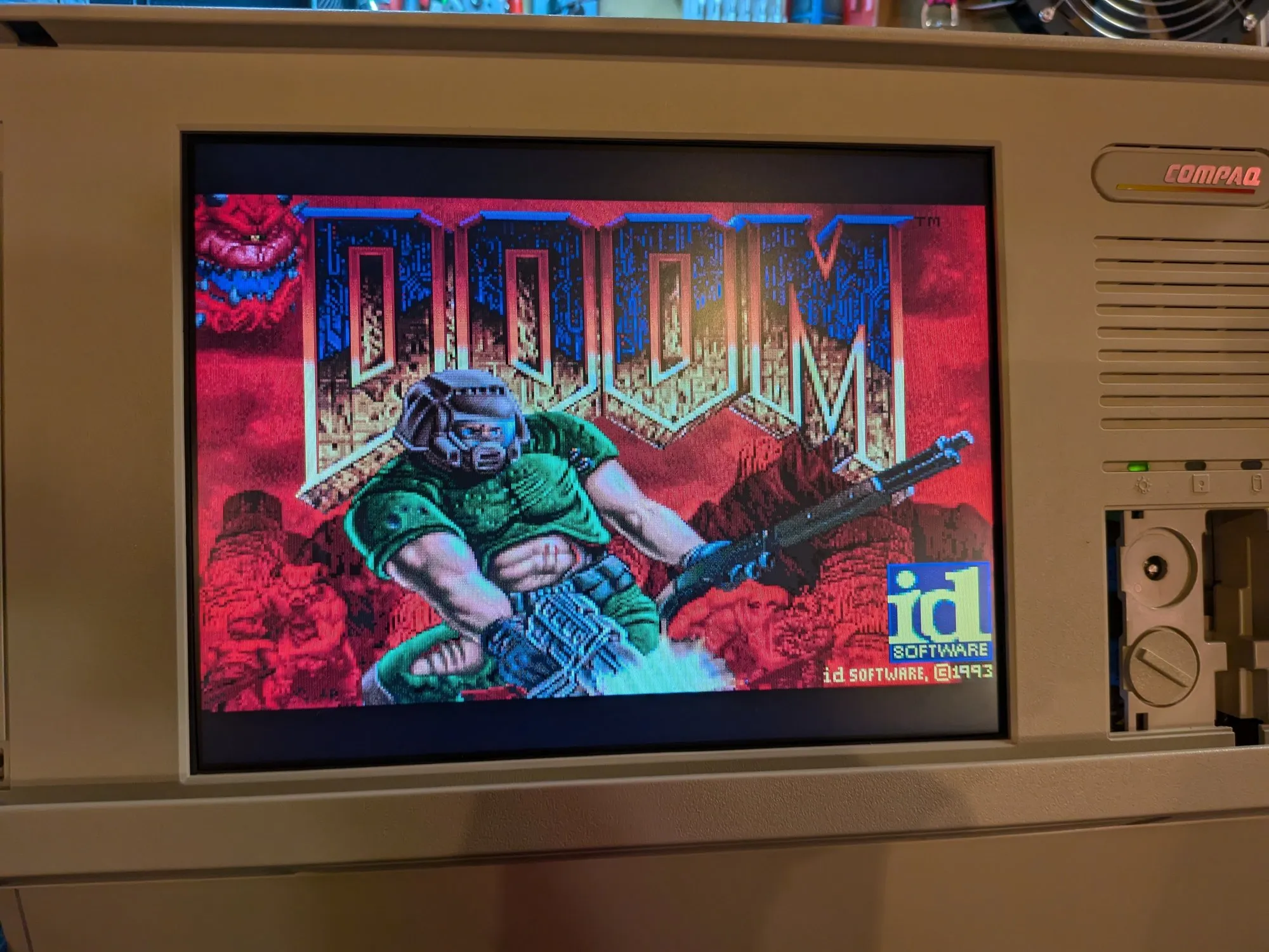
It’s not a vintage computing project until you run DOOM on it. I don’t make the rules - the retro community bylaws are very clear on this. No DOOM screenshot, no credibility.
Resources
- DOSReloaded Forum Thread (German): Beckenrandschwimmer’s original write-up with oscilloscope measurements and circuit diagrams
- VCFed Forum Thread: My restoration thread with discussion and community Q&A
- 40-pin to 31-pin TTL cable (eBay): Adapter cable used for wiring
- Dual CCFL Inverter Board (eBay): Backlight inverter used